|
Features
|
Capability
|
Description
|
Patterns
|
|
Layer count
|
1-32 Layers
|
The number of copper layers in the PCB
|
|
|
Controlled Impedance
|
4/6/8/10/12/14/16/18/20/.../32 layers
|
||
|
Material
|
FR-4
|
Grade A laminates from suppliers including Nan Ya, KB, Shengyi and etc.
|
 |
|
Aluminum-Core
|
 |
||
|
Copper-Core
|
 |
||
|
RF PCB
|
 |
||
|
FR-4 Dielectric Constants
|
4.5 (2-Layer PCB)
|
7628 Prepreg 4.4
3313 Perpreg 4.1
2216 Perpreg 4.16
|
|
|
Maximum Dimensions
|
FR4 PCB: 670 × 600 mm
Rogers / PTFE Teflon PCB: 590 × 438 mm
Aluminum PCB: 602 × 506 mm
Copper PCB: 480 × 286 mm
|
These limits apply to PCBs with thickness ≥ 0.8 mm. The thinner FR4 PCBs are 500 × 600 mm maximum.
2-layer FR4 PCBs can reach a maximum size of 1020 × 600 mm.
|
 |
|
Minimum Dimensions
|
Regular: 3 × 3 mm. Castellated / Plated Edges: 10 × 10 mm.
|
These limits apply to PCBs with thickness ≥ 0.6 mm. Manual review required for thinner PCBs. Panelization is recommended for small-sized boards.
|
|
|
Dimension Tolerance
|
±0.1mm
|
±0.1mm(Precision) and ±0.2mm(Regular) for CNC routing, and ±0.4mm for V-scoring
|
|
|
Thickness
|
0.4 - 4.5 mm
|
Thickness for FR4 are: 0.4/0.6/0.8/1.0/1.2/1.6/2.0 mm (2.5 mm and above are for 12+ layer PCBs only)
|
 |
|
Thickness Tolerance
(Thickness≥1.0mm)
|
± 10%
|
e.g. For the 1.6mm board thickness, the finished board thickness ranges from 1.44mm(T-1.6×10%) to 1.76mm(T+1.6×10%)
|
|
|
Thickness Tolerance
(Thickness<1.0mm)
|
± 0.1mm
|
e.g. For the 0.8mm board thickness, the finished board thickness ranges from 0.7mm(T-0.1) to 0.9mm(T+0.1).
|
|
|
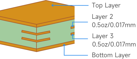
Finished Outer Layer Copper
|
1 oz / 2 oz (35um / 70um)
|
Finished copper weight of outer layer is 1oz or 2oz.
|
 |
|
Finished Inner Layer Copper
|
0.5 oz / 1 oz / 2 oz (17.5um / 35um / 70um)
|
Finished copper weight of inner layer is 0.5oz by default.
|
 |
|
Soldermask
|
Green, Purple, Red, Yellow, Blue, White, and Black.
|
We use LPI (Liquid Photo Imageable) solder mask. This is the most common type of mask used today. Heat-cured ink soldermask is usually found on low-cost, single-sided PCBs.
|
|
|
Surface Finish
|
HASL (leaded / lead-free), ENIG, OSP (copper core boards only)
|
FR4 has all three finishes available, 6+ layers and RF boards only have ENIG.
Aluminium core boards only have HASL. Copper core boards only have OSP.
|
Drilling
|
Features
|
Capability
|
Description
|
Patterns
|
|
Drill Diameter
|
1-layer: 0.3 – 6.3 mm
2-layer: 0.3 – 6.3 mm
Multilayer: 0.15 – 6.3 mm
|
Holes with diameter ≥ 6.3 mm are CNC routed from a smaller drilled hole.
Min. drill diameter for 2- or more-layer PCBs is 0.3 mm (more costly!)
Min. drill diameter for aluminum-core PCBs is 0.65 mm
Min. drill diameter for copper-core PCBs is 1.0 mm
|
|
|
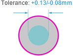
Hole size Tolerance (Plated)
|
Through-holes: +0.13 / -0.08 mm
Press-fit holes:±0.05 mm (multilayer ENIG boards only – mention the specific holes in PCB Remark)
|
e.g. for the 0.6mm hole size, the finished hole size between 0.52mm to 0.73mm is acceptable.
|
 |
|
Hole size Tolerance (Non-Plated)
|
±0.2mm
|
e.g. for the 1.00mm Non-Plated hole, the finished hole size between 0.80mm to 1.20mm is acceptable.
|
 |
|
Average Hole Plating Thickness
|
18μm
|
||
|
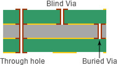
Blind/Buried Vias
|
Not supported
|
Currently we don't support Blind/Buried Vias, only make through holes.
|
 |
|
Min. Via hole size/diameter
|
0.15mm / 0.25mm
|
1-layer (NPTH only): 0.3 mm hole size / 0.5 mm via diameter
2-layer: 0.30mm hole size / 0.50mm via diameter
Multilayer: 0.15 mm hole size / 0.25 mm via diameter
① Via diameter should be 0.1mm(0.15mm preferred) larger than Via hole size.
② Preferred Min. Via hole size: 0.2mm
|
 |
|
Min. Non-plated holes
|
0.50mm
|
Please draw NPTHs in the mechanical layer or keep out layer.
|
 |
|
Min. Plated Slots
|
0.5mm
|
The minimum plated slot width is 0.5mm, which is drawn with a pad.
|
 |
|
Min. Non-Plated Slots
|
1.0mm
|
The minimum Non-Plated Slot Width is 1.0mm, please draw the slot outline in the mechanical layer(GML or GKO)
|
 |
|
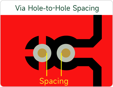
Via Hole-to-Hole Spacing
|
0.2mm
|
 |
|
|
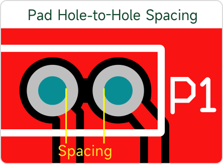
Pad Hole-to-Hole Spacing
|
0.45mm
|
 |
|
|
Min. Castellated Holes
|
0.60mm
|
Castellated holes are metalized half-holes on PCB edges, commonly used on daughter boards to be soldered onto carrier PCBs.
① Hole diameter (Φ): ≥ 0.6 mm
② Hole to board edge (L): ≥ 1 mm
③ Hole to hole (D): ≥ 0.6 mm
④ Min. PCB size:10 × 10 mm
⑤ Min. PCB thickness: 0.6 mm
|
 |
|
10 x 10mm
|
Plated edges are copper-plated and ENIG treated. HASL is not supported.
① Min. PCB size: 10 × 10 mm
② Min. PCB thickness: 0.6 mm
③ At least 3 breaks (more for larger PCBs) in the edge plating are required for support tab connections
|
 |
|
|
Rectangular Holes / Slots
|
Not supported
|
Rectangular holes and slots without rounded corners are not supported. For non-plated slots, the recommended minimum size is 3 × 3 mm.
|
 |
Traces
|
Features
|
Capability
|
Description
|
Patterns
|
|
Min. track width and spacing (1 oz)
|
0.10 / 0.10 mm (4 / 4 mil)
|
1- and 2-layer: 0.10 / 0.10 mm (4 / 4 mil)
Multilayer: 0.09 / 0.09 mm (3.5 / 3.5 mil). 3 mil is acceptable in BGA fan-outs.
|
 |
|
Min. track width and spacing (2 oz)
|
0.16 / 0.16 mm (6.5 / 6.5 mil)
|
2-layer: 0.16 / 0.16 mm (6.5 / 6.5 mil)
Multilayer: 0.16 / 0.20 mm (6.5 / 8 mil)
|
|
|
Track width tolerance
|
±20%
|
e.g. For a 0.1 mm track, the finished track width ranges from 0.08 and 0.12 mm.
|
|
|
PTH annular ring
|
≧0.20mm
|
2-layer:
1 oz: Recommended 0.25 mm or above; absolute minimum 0.18 mm
2 oz: 0.254 mm or above
Multilayer:
1 oz: Recommended 0.20 mm or above; absolute minimum 0.15 mm
2 oz: 0.254 mm or above
|
 |
|
NPTH pad annular ring
|
≧0.45mm
|
Recommended 0.45 mm or more. This is to allow a 0.2 mm ring of copper to be removed around the hole for the sealing film to attach. Pad sizes smaller than the recommended value can result in the annular ring being very thin or completely missing.
|
|
|
0.25mm
|
① BGA pad diameter ≥ 0.25 mm
② BGA pad to trace clearance ≥ 0.1 mm (min. 0.09 mm for multilayer boards)
③ Vias can be placed within BGA pads using filled and plated-over vias
|
 |
|
|
Trace coils
|
0.15/0.15mm
|
Minimum trace width/clearance: 0.15/0.15mm, when traces are covered by solder mask (1oz).
Minimum trace width/clearance: 0.25/0.25mm, when traces are NOT covered by solder mask (1oz). ENIG only(high risk of short circuit with HASL)
|
 |
|
Hatched grid width and spacing
|
0.25 mm
|
 |
|
|
Same-net track spacing
|
0.25mm
|
 |
|
|
Inner layer via hole to copper clearance
|
0.2mm
|
|
|
|
Inner layer PTH pad hole to copper clearance
|
0.3mm
|
||
|
Pad to track clearance
|
0.1mm
|
Min. 0.1 mm (stay well above if possible). Min. 0.09 mm locally for BGA pads
|
 |
|
SMD pad to pad clearance (different nets)
|
0.1mm
|
 |
|
|
Pad to Pad clearance(Different nets)
|
0.45mm
|
|
|
|
Via to Track
|
0.2mm
|
 |
|
|
PTH to Track
|
0.275mm
|
||
|
NPTH to Track
|
0.2mm
|
 |
Soldermask
|
Features
|
Capability
|
Description
|
Patterns
|
|
Soldermask Expansion
|
0.038mm
|
2-layer: 0.038 mm expansion on each side of a pad. Keep at least 0.05 mm clearance between soldermask openings and neighboring traces.
Multilayer: No expansion required
|
 |
|
0.10mm
|
2-layer (1 oz):
Min. pad spacing: 0.20 mm (green, red, yellow, blue, purple)
Min. pad spacing: 0.23 mm (black, white)
Multilayer (1 oz):
Min. pad spacing: 0.10 mm (green, red, yellow, blue, purple)
Min. pad spacing: 0.13 mm (black, white)
|
 |
|
|
Plugged vias
|
Filled with soldermask
|
Vias are filled with soldermask for an opaque finish.
① Filled vias must not have soldermask openings on either side
② Filled vias should have ≥ 0.35 mm clearance from other soldermask openings (e.g. pads)
③ Filled vias must be no wider than 0.5 mm diameter
|
 |
|
JLCPCB Via-in-Pad Process
|
Epoxy Filled & Capped
Copper paste Filled&Capped
|
Vias are filled with epoxy resin or copper paste and then plated over to achieve an opaque and smooth finish.
① Vias are filled and plated over. Choose copper paste filling for applications requiring high thermal conductivity.
② This process is the default for 6-layer and above multilayer boards.
③ Compatible with via diameters from 0.15 to 0.5 mm.
|
 |
|
Solder mask dielectric constant
|
3.8
|
|
|
|
Solder mask ink thickness
|
≥ 10μm
|
|
Features
|
Capability
|
Description
|
Patterns
|
|
Minimum Line Width
|
6 mil (0.153mm)
|
Characters width less than 6mil(0.153mm) will be unidentifiable.
|
 |
|
Minimum text height
|
40 mil (1.0mm)
|
Characters height less than 40 mil(1.0mm) will be unidentifiable.
|
 |
|
Character width to height ratio
|
1:6
|
The preferred ratio of width to height is 1:6.
|
 |
|
Hollow-carved Character width to height ratio
|
1:6
|
The preferred ratio of width to height is 1:6
|
 |
|
Pad To Silkscreen
|
0.15mm
|
The Minimum Distance Between Pad and Silkscreen is 0.15mm.
|
 |
|
Features
|
Capability
|
Description
|
Patterns
|
|
Routed
|
0.2mm
|
① Copper clearance from routed board edges: ≧0.2 mm
② Copper clearance from routed slots: ≧0.2 mm
③ Dimension tolerance for routed board edges: ±0.2 mm (regular precision); ±0.1 mm (high precision)
|
 |
|
0.4mm
|
① Copper clearance from V-cut board edges: ≧0.4 mm
② Dimension tolerance for V-cut board edges: ±0.4 mm. PCB thickness ≥ 0.6 mm
③ Zero panel board spacing by default. Alternatively, V-cut along one direction with no spacing and route along the other direction with 1.6 or 2 mm board spacing.
④ Min. panel dimensions: 70 × 70 mm; max. panel dimensions: 475 × 475 mm
⑤ V-cut groove angle: 25°
|
 |
|
|
0.2mm
|
① Copper clearance from non-mouse-bite board edges: ≧0.2 mm
② Dimension tolerance for non-mouse-bite board edges: ±0.2 mm (regular precision); ±0.1 mm (high precision)
③ Panel board spacing: 1.6 or 2 mm
④ Serrated edges will remain after depanelization
⑤ Minimum tooling edge width: 3 mm. For SMT assembly at JLCPCB, use 5 mm tooling edges, 2 mm tooling holes, and 1 mm fiducials centered at 3.85 mm from the panel edges.
|
|
|
|
Panelization with space
|
2mm
|
The spacing between boards should be ≥ 2 mm, as narrow spacing results in difficulties for routing and V-cut.
|
 |
|
Panel of Circular PCBs
|
≥20mmx20mm
|
The single round board size should be≥20mmx20mm when choose panel by JLCPCB.
Panelize with stamp holes and add tooling strips on four board edges
|
 |
'HW' 카테고리의 다른 글
| SMD 저항 사이즈 표 (0) | 2025.04.09 |
|---|---|
| <개발> 리눅스 하드웨어 개발 시 부품 선정 방법. (0) | 2025.04.09 |
| 탄탈, 세라믹 캐패시터 차이점 (0) | 2025.04.07 |
| JLCPCB 임피던스 계산기 (0) | 2025.04.04 |
| KI CAD 거버 설정 방법 (0) | 2025.04.01 |


